The analysis of this circuit is essentially the same as that of an inverting amplifier except that the noninverting input of the op-amp is at a voltage equal to a fraction of V 2 rather than being connected directly to ground. If all the resistor values are equal this amplifier will have a differential voltage gain of 1.

Distributed Rf Amplifier Designs For Ultra Wideband Applications Mini Circuits Blog
Below you can see the block diagram of a basic PWM Class-D amplifier just like the one that we are building.

. Design and Simulation of Synthesizers PDF - 15MB 19 Basics of Wireless Communication 20 Performance Measures of Wireless Communication. MSG 20 dB. 12 where xdxd xd ds ds d C R CR 1 1 w w Using 9-12 the image impedance and propagation factor can be calculated using 4 and 5.
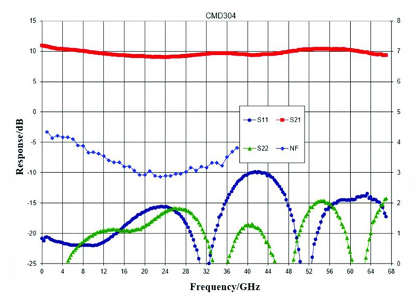
S-parameters and noise figure versus frequency for the CMD304 distributed amplifier. The general design considerations included in this paper are. It is an extension of the original Distributed Amplifier example to now include Parametric Layout.
For comparison the class B amplifier can only achieve a maximum efficiency of 785 in theory. W w w ww. Example Amplifier Design Design a single stage amplifier with G 14 dB and input match.
The DA stability is compromised when using multi-stage amplifiers as gain stage. These expressions are plotted in figures 6 7 and 8. Based on the requirement of the gain in the circuit one or more amplifier devices are used.
G m variations with freq. A CMoy pocket amp with a decent but unexceptional op-amp followed by a gang of high-spec PIMETA v2s might well sound better than if the PIMETAs had the same op-amp as the CMoys. Let me try to find it.
Distributed Ampli er v s v o Zd Z g M1 M2 M3 M4 dZ d gZ g g d Z Z g The goal is to convert the lumped ampli er into a distributed structure. Select load far away from instability region. The CMD304 for example is a DC-67 GHz distributed amplifier with a flat gain response with respect to frequency as shown in Figure 3.
Also plot load stability. High G m value is desired to enhance DA gain. S-parameters and noise figure versus frequency for the CMD192C5 distributed amplifier.
Class D Audio Amplifier Design Class D Amplifier Introduction Gate Driver MOSFET Package Design Example Theory of Class D operation topology comparison How to drive the gate key parameters in gate drive stage How to choose tradeoff relationships loss calculation Importance of layout and package new packaging technology. To employ the distributed amplification technique for the design of ultra-wide-band low-noise amplifiers the poor noise performance of the conventional distributed amplifiers DAs needs to. 201 shows a class A common emitter amplifier but without its component values.
Distributed amplifier tutorial I have tried to design some distributed amplifier using the book by Virdee. The concept of distributed amplification was deeply investigated and some of the limitations which degraded the performance of such amplifiers have been presented. A distributed amp is a clever way to provide enormous bandwidths as much as 100 GHz.
Enhancement of Broadband Amplifiers Narrowband Amplifiers 7 Noise Modeling in Amplifiers 8 Noise Figure Impact of Amplifier Nonlinearities 9 Low Noise Amplifiers 10 Mixers 11 Voltage Controlled Oscillators. Design issues in DA gain stages. 2Amplifiers one or in stages.
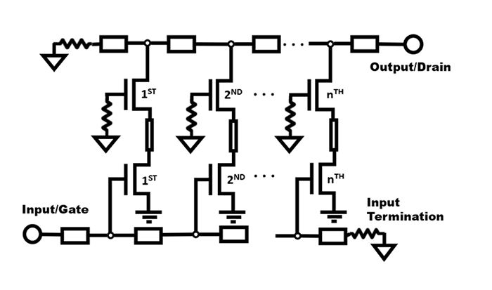
The theory behind the distributed amplifier is that a number of FETs at least two but more typically four five or six are fed by a periodic structure at. Both transmission lines need to be properly. I have done it for few years.
The plots are generated. Consequently the focus of this thesis is upon the application of distributed integrated circuit methodologies towards the realization of a distributed broadband amplifier in a commercial CMOS process technology. Some distributed amplifiers can operate down to DC as well so they are used as opto-electronic amps.
BW of DA is limited by BW of G m stages. Noise contribution of G m stage should be low. Since input must be matched lets select the load for gainstability.
Affect the DA gain flatness. Class A Amplifier Design Introduction to Amplifier Design Basic design process. Example of a 100W Class D Amplifier ENABLE 6 V 6 V 20 V 20 V 47 Ω 10 µF R8 C11 Optional switching noise filter Demodulation LPF Startup resister High-side OCP Bootstrap floating supply charging path Low-side OCP Dead-time Feedback resistor 2nd order integrator Input resistor VAA supply VSS supply DC blocking capacitor Bootstrap floating supply capacitor.
Because of this the amplifier does not generate a lot of heat and does not require a big heat sink like linear class AB amplifiers do. Back-off by 6 dB and plot Gp 14 dB circles. The CMD275P4 is an example of an extremely broadband low phase noise amplifier.
Distributed Amplifier This example demonstrates a MMIC design of a distributed amplifier with a flat gain of about 12dB from about 2GHz to 10GHz. If multiple devices are used they are connected either in parallel or in. I dont know this approach will be good up to 10 GHz or not.
A wasteful but easy and functional way to build such a distribution amp is to buildbuy K1 headphone amps set K of them to a gain of 1 and build an octopous cable between the. Following are the RF power amplifier stages or modules. This module shows how to simply calculate the values needed to make a working amplifier that has correct class A bias as described in Amplifier.
The idea is to take a xed g m transistor width W and split it into parallel ngers that are embedded into a transmission line at the gate and drain. Out of the two parts of this thesis the first part addresses the design and implementation of a distributed amplifier on PCB. In Virdees book they use a chip FET and use wire bound as inductors.
I do have design examples using ADS. Input degernation with distributed amplifier at the upper 3 - dB design frequency of the amplifier Suppose we apply degeneration to make G 11new G 22new max 11 22 2 2111 22 221 2 0 221 2. Used to match the amplifier device with input 50 Ohm impedance line.
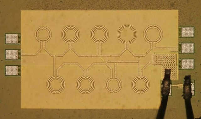
On-chip spiral inductors were utilized in on-chip bias circuitry. When compared to a similar broadband part designed on a pHEMT process this component which was developed on an HBT process shows about a 20 dBcHz improvement in phase noise at a 10 kHz offset. The effect of.
MTT 121998 murthy Electronics letters 2003. The low-pass amplifiers can be made to have a uniform frequency response from dc to frequencies as high as several hundred Mc using commercially available tubes. Faculties and often novel design capabilities for a given IC process.
The distributed amplifier provides means for designing amplifiers either of the low-pass or band-pass types.

Distributed Rf Amplifier Designs For Ultra Wideband Applications Mini Circuits Blog

Distributed Rf Amplifier Designs For Ultra Wideband Applications Mini Circuits Blog

Microwaves101 Distributed Amplifiers
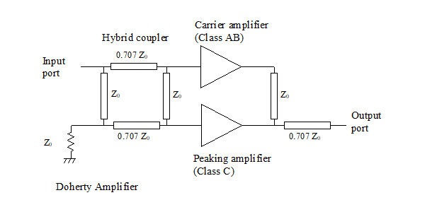
Microwaves101 Doherty Amplifiers
Distributed Rf Amplifier Designs For Ultra Wideband Applications Mini Circuits Blog
Distributed Amplifiers Are A Unique Circuit In High Frequency Microwave Engineering Qorvo
Microwaves101 Distributed Amplifiers
Distributed Amplifiers Are A Unique Circuit In High Frequency Microwave Engineering Qorvo
0 comments
Post a Comment